
Microelectromechanical systems (MEMS), also written as microelectromechanical systems (or microelectronic and microelectromechanical systems). And the related Microsystems and micro mechatronics. Constitute the technology of microscopic devices, particularly those with moving parts. They merge at the nanoscale into Nanoelectromechanical systems (NEMS) and nanotechnology . MEMS are also know as micromachine in Japan. And Microsystems technology (MST) in Europe.
MEMS are make up of components between 1 and 100 micrometers in size (i.e., 0.001 to 0.1 mm). And MEMS devices range in size from 20 micrometers to one millimeter (i.e., 0.02 to 1.0 mm). Mm), although the components are arrange in arrays (eg. Digital micromirrors devices) can be greater than 1000 mm 2. They consist of a central unit. That processes data (an integrated circuit chip such as a microprocessor). and various components that interact with the environment (such as microsensors). Due to the large surface area to volume ratio of MEMS. The forces produced by the Stollschulte electromagnetism. (for example, electrostatic charges and magnetic moments ). And fluid dynamics (for example, surface tension and viscosity ). Are more important design considerations. than with larger-scale mechanical devices. MEMS technology is distinguish from molecular nanotechnology. Or molecular electronics in that the latter must also consider surface chemistry.
The potential of very small machines was appreciate before the technology. That could make them exist (see, for example. Richard Feynman’s famous 1959 lecture there’s Plenty of Room at the Bottom). MEMS became practical once they could be make. Using modified semiconductor device fabrication technologies. used to make electronics. These include molding and plating, wet etching (KOH, TMAH). And dry etching (RIE and DRIE), electrical discharge machining (EDM). And other technologies capable of manufacturing small devices.
History
MEMS technology has its roots in the silicon revolution. Dating back to two major silicon semiconductor inventions of 1959. Robert Noyce’s monolithic integrated circuit (IC) chip at Fairchild Semiconductor. And the MOSFET (field effect metal-oxide semiconductor transistor or MOS transistor). By Mohamed M. Atalla and Dawon Kahng at Bell Labs. MOSFET scaling, the miniaturization of MOSFETs on IC chips. Led to the miniaturization of electronics. (as predicted by Moore’s law and Dennard scaling). This laid the foundation for the miniaturization of mechanical systems. With the development of micromachining technology based on silicon semiconductor technology. As engineers began to realize that silicon chips and MOSFETs could interact. And communicate with the environment and process things like chemicals, motion, and light. One of the first silicon pressure sensors was micromachine by Honeywell in 1962.
An early example of a MEMS device is the resonant gate transistor. an adaptation of the MOSFET, developed by Harvey C. Nathanson in 1965. Another early example is the resonistor. A monolithic electromechanical resonator patented by Raymond J. Wilfinger in 1966 and 1971. During the 1970s through the early 1980s. Various MOSFET microsensors were develop to measure physical, chemical, biological, and environmental parameters.
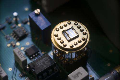
Types
There are two basic types of MEMS switching technology: capacitive and ohmic. A capacitive MEMS switch is develop using a moving plate or sensing element. Which changes capacitance. Ohmic switches are control by control cantilevers. Ohmic MEMS switches can fail. Due to metal fatigue of the MEMS actuator (cantilever) and contact wear. As the cantilevers can deform over time.
Materials for MEMS Fabrication
MEMS fabrication evolved from process technology in semiconductor device fabrication. That is, the basic techniques are material layer deposition. Photolithography patterning, and etching to produce the required shapes.
Silicon
Silicon is the material use to create. Most of the integrated circuits use in consumer electronics in modern industry. Economies of scale, the ready availability of high-quality. Inexpensive materials, and the ability to incorporate. Electronic functionality make silicon attractive for a wide variety of MEMS applications. Silicon also has important advantages derive from the properties of its materials. In single-crystal form, silicon is a perfect Hookean material. Meaning that when it is flex there is no hysteresis and thus almost no power dissipation. As well as achieving y repeatable motion. this also makes the silicon very reliable as it suffers from very little fatigue. And can have a service life in the range of billions to trillions of cycles without breaking. Silicon-based semiconductor nanostructures are becoming important in the field of microelectronics. And MEMS in particular. Silicon nanowires, made by thermal oxidation of silicon. Are of greatest interest in electrochemical conversion and storage. Including nanowire batteries and photovoltaic systems.
Polymers
Although the electronics industry provides economies of scale for the silicon industry. Crystalline silicon remains a complex and expensive material to produce. So, polymers can be produce in large volumes. With a wide variety of material characteristics. MEMS devices can be make from polymers by processes such as injection molding. Stamping, or stereo lithography and are particularly well suit for microfluidics applications. Such as disposable blood test cartridges.
Metals
Metals can also be use to create MEMS elements. While metals do not have some of the advantages. That silicon exhibits mechanical properties. When used within their limitations metals can exhibit very high degrees of reliability. Metals can be deposit by electroplating, evaporation, and sputtering processes. used metals include gold, nickel, aluminum, copper, chrome, titanium, tungsten, platinum, and silver.